

Online message
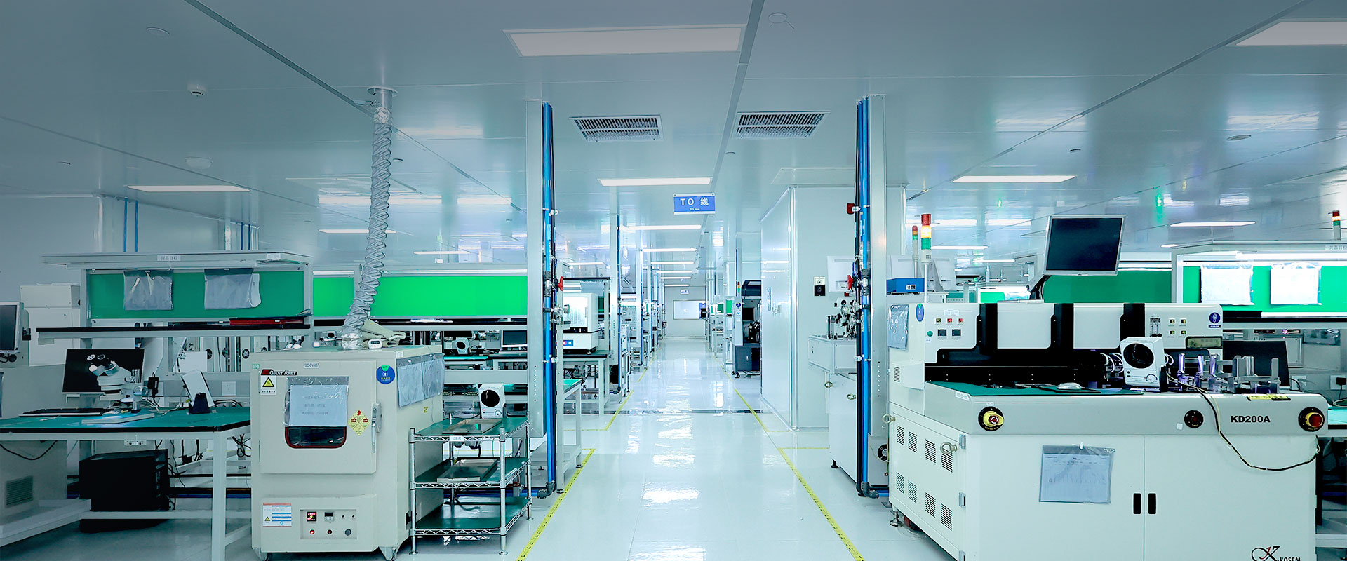
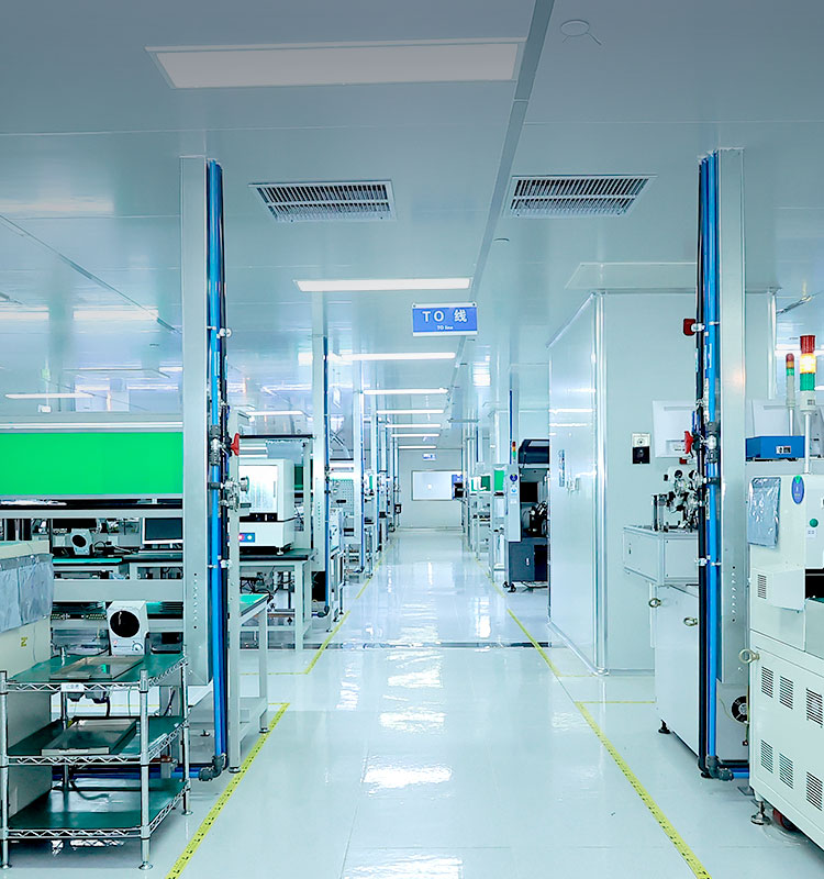
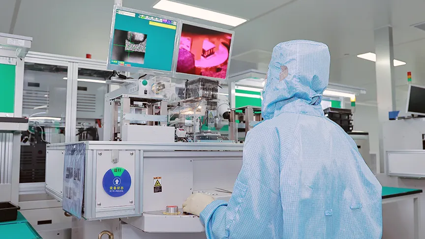
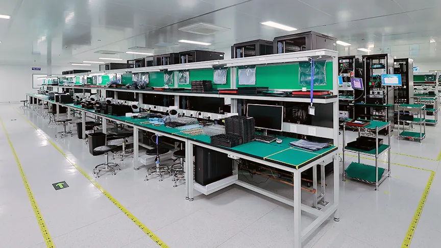
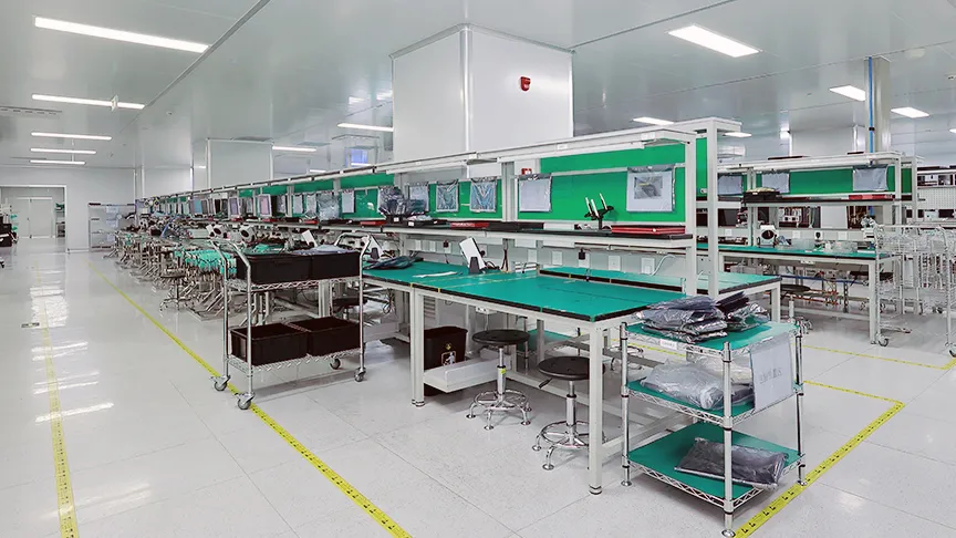
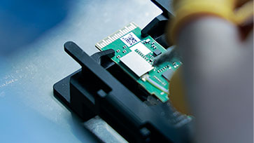
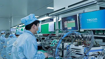
The production base in Suzhou has a 12,000+ square meter dust-free workshop of ten-thousand grade, providing a one-stop production process from devices, COB, assembly to testing.
It has four packaging platforms: coaxial packaging, multimode COB, micro-optics, and COB + hybrid integration platform.From chips, devices, modules to applications: Relying on independent innovation and focusing on high-speed data transmission optoelectronic products.

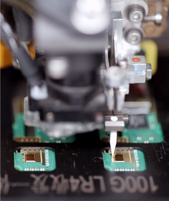
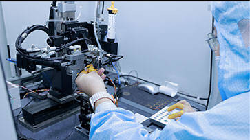
Pull-push force test
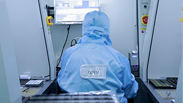
SEM inspection
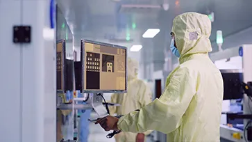
Crater test
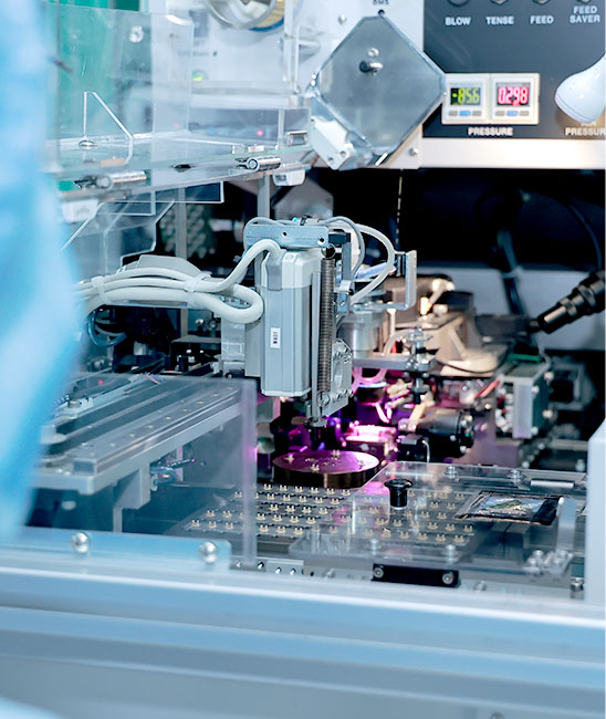
Wire-bonding parameter optimization
| Leg | 1 | 2 | 3 | 4 | 5 | 6 | 7 | 8 | 9 |
| Power | 300 | 300 | 320 | 320 | 280 | 300 | 280 | 320 | 280 |
| Time | 10 | 15 | 20 | 10 | 15 | 20 | 10 | 15 | 20 |
| Force | 10 | 15 | 10 | 15 | 10 | 20 | 10 | 15 | 20 |
| Ball Shear | 26.744 | 26.488 | 28.028 | 36.644 | 28.488 | 36.524 | 27.566 | 35.532 | 29.842 |
| Wire Pull | 13.724 | 14.858 | 14.964 | 14.396 | 14.024 | 13.53 | 11.43 | 13.292 | 11.204 |
| Stitch Pull | 13.874 | 14.638 | 14.222 | 14.342 | 14.04 | 14.23 | 13.722 | 14.388 | 13.52 |
| Ball Size | 63 | 64 | 63 | 65 | 62 | 63 | 63 | 64 | 62 |
| Ball Size | 0 | 0 | 0 | 0 | 0 | 0 | 0 | 0 | 0 |


Online message
Building 6,No.199,Guanpu Road,Guoxiang,Wuzhong Economic Development Area,Suzhou
Tel:+86-512-66257838
Sales E-Mail: sales@terabitcom.com
Technical Support E-Mail: support@terabitcom.com